BSP300
SIPMOS ® Small-Signal Transistor
• N channel
• Enhancement mode
• Avalanche rated
• VGS(th)= 2.0... 4.0 V
• Pb-free lead plating; RoHS compliant
• Qualified according to AEC Q101
Pin 1
Pin 2
G
D
Type
VDS
ID
RDS(on)
Package
Marking
BSP300
800 V
0.19 A
20 Ω
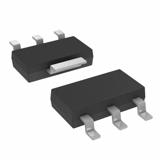
PG-SOT223
BSP300
Type
BSP300
RoHS compliant
Yes
Pin 3
Pin 4
S
D
Tape and Reel Information Packaging
L6327
Dry
Maximum Ratings
Parameter
Symbol
Continuous drain current
ID
TA = 25 °C
Values
Unit
A
0.19
DC drain current, pulsed
IDpuls
TA = 25 °C
0.76
Avalanche energy, single pulse
mJ
E AS
ID = 0.8 A, VDD = 50 V, RGS = 25 Ω
L = 105 mH, Tj = 25 °C
36
Gate source voltage
V GS
Power dissipation
P tot
TA = 25 °C
V
W
1.8
ESD Class
JESD22-A114-HBM
Rev 2.1
± 20
Class 1a
Page 1
2008-03-26
�BSP300
Maximum Ratings
Parameter
Symbol
Values
Chip or operating temperature
Tj
-55 ... + 150
Storage temperature
Tstg
-55 ... + 150
Thermal resistance, chip to ambient air 1)
RthJA
≤ 70
Thermal resistance, junction-soldering point 1)
RthJS
≤ 14
DIN humidity category, DIN 40 040
Unit
°C
K/W
E
IEC climatic category, DIN IEC 68-1
55 / 150 / 56
1) Transistor on epoxy pcb 40 mm x 40 mm x 1,5 mm with 6 cm2 copper area for drain connection
Electrical Characteristics, at Tj = 25°C, unless otherwise specified
Parameter
Symbol
Values
min.
typ.
Unit
max.
Static Characteristics
Drain- source breakdown voltage
V GS = 0 V, ID = 0.25 mA, Tj = 25 °C
Gate threshold voltage
800
-
-
2
3
4
V GS(th)
V GS=V DS, ID = 1 mA
Zero gate voltage drain current
V
V (BR)DSS
µA
IDSS
V DS = 800 V, V GS = 0 V, Tj = 25 °C
-
0.1
1
V DS = 800 V, V GS = 0 V, Tj = 125 °C
-
10
100
Gate-source leakage current
V GS = 20 V, VDS = 0 V
Drain-Source on-state resistance
-
10
100
Ω
RDS(on)
V GS = 10 V, ID = 0.19 A
Rev 2.1
nA
IGSS
-
Page 2
15
20
2008-03-26
�BSP300
Electrical Characteristics, at Tj = 25°C, unless otherwise specified
Parameter
Symbol
Values
min.
typ.
Unit
max.
Dynamic Characteristics
Transconductance
V DS≥ 2 * ID * RDS(on)max, ID = 0.19 A
Input capacitance
0.06
pF
-
170
230
-
20
30
-
10
15
Crss
V GS = 0 V, V DS = 25 V, f = 1 MHz
Turn-on delay time
-
Coss
V GS = 0 V, V DS = 25 V, f = 1 MHz
Reverse transfer capacitance
0.27
Ciss
V GS = 0 V, V DS = 25 V, f = 1 MHz
Output capacitance
S
gfs
ns
td(on)
V DD = 30 V, VGS = 10 V, ID = 0.25 A
RGS = 50 Ω
Rise time
-
7
11
-
16
24
-
27
36
-
21
28
tr
V DD = 30 V, VGS = 10 V, ID = 0.25 A
RGS = 50 Ω
Turn-off delay time
td(off)
V DD = 30 V, VGS = 10 V, ID = 0.25 A
RGS = 50 Ω
Fall time
tf
V DD = 30 V, VGS = 10 V, ID = 0.25 A
RGS = 50 Ω
Rev 2.1
Page 3
2008-03-26
�BSP300
Electrical Characteristics, at Tj = 25°C, unless otherwise specified
Parameter
Symbol
Values
min.
typ.
Unit
max.
Reverse Diode
Inverse diode continuous forward current
TA = 25 °C
Inverse diode direct current,pulsed
-
-
0.76
V
1
1.4
ns
trr
-
95
µC
Qrr
V R = 30 V, IF=lS = 0 , diF/dt = 100 A/µs
Rev 2.1
0.19
-
V R = 30 V, IF=lS = 0 , diF/dt = 100 A/µs
Reverse recovery charge
-
V SD
V GS = 0 V, IF = 0.38 A, Tj = 25 °C
Reverse recovery time
ISM
TA = 25 °C
Inverse diode forward voltage
A
IS
-
Page 4
0.25
-
2008-03-26
�BSP300
Power dissipation
Ptot = ƒ(TA)
Ptot
Drain current
ID = ƒ(TA)
parameter: VGS ≥ 10 V
2.0
0.20
W
A
1.6
ID
0.16
1.4
0.14
1.2
0.12
1.0
0.10
0.8
0.08
0.6
0.06
0.4
0.04
0.2
0.02
0.0
0.00
0
20
40
60
80
100
120
°C
160
0
20
40
60
80
100
TA
Safe operating area
ID = ƒ(VDS)
parameter: D = 0.01, TC = 25°C
10 0
120
°C
160
TA
Transient thermal impedance
Zth JA = ƒ(tp )
parameter: D = tp / T
10 2
t = 760.0µs
p
1 ms
/I
D
K/W
10 1
=V
DS
A
10 ms
DS
(on
)
ID
10 0
R
10 -1
ZthJC
10 -1
D = 0.50
10 -2
0.20
10 -2
0.10
10 -3
0.05
single pulse
10 -4
0.02
0.01
DC
10 -3
0
10
10
1
10
2
V 10
10 -5
-8
-7
-6
-5
-4
-3
-2
-1
0
10
10
10
10
10
10
10
10 s 10
3
VDS
Rev 2.1
tp
Page 5
2008-03-26
�BSP300
Typ. output characteristics
ID = ƒ(VDS)
parameter: tp = 80 µs , Tj = 25 °C
0.45
Typ. drain-source on-resistance
RDS (on) = ƒ(ID)
parameter: tp = 80 µs, Tj = 25 °C
l
65
Ptot = 2W
Ω
kjihg
f e
A
b
55
VGS [V]
ID
a
d
0.35
0.30
c
0.25
0.20
0.15
a
4.0
b
4.5
c
5.0
d
5.5
e
6.0
f
6.5
g
7.0
h
7.5
i
8.0
j
9.0
b k
10.0
l
20.0
RDS (on)
50
45
40
35
30
c
25
20
15
0.10
10
a
0.05
k
VGS [V] =
5
0.00
d
e gh f
ji
a
4.5
4.0
b
5.0
c
5.5
d
6.0
e
f
6.5 7.0
g
7.5
h
i
j
k
8.0 9.0 10.0 20.0
0
0
4
8
12
16
V
24
0.00 0.04 0.08 0.12 0.16 0.20 0.24 0.28 A 0.34
VDS
ID
Typ. transfer characteristics ID = f(VGS)
Typ. forward transconductance gfs = f (ID)
parameter: tp = 80 µs
parameter: tp = 80 µs,
VDS≥ 2 x ID x RDS(on)max
V DS≥2 x ID x RDS(on)max
I
1.0
0.50
A
S
0.8
g
D
0.40
fs
0.7
0.35
0.6
0.30
0.5
0.25
0.4
0.20
0.3
0.15
0.2
0.10
0.1
0.05
0.0
0.00
0
1
2
3
4
5
6
7
8
V
V
Rev 2.1
1.0
1
10
0.0
0.1
0.2
0.3
0.4
0.5
0.6
A
0.8
I
GS
D
Page 1
6
2005-10-27
2008-03-26
�BSP300
Drain-source on-resistance
RDS (on) = ƒ(Tj )
parameter: ID = 0.19 A, VGS = 10 V
Gate threshold voltage
VGS (th) = ƒ(Tj )
parameter: VGS = VDS, ID = 1 mA
50
4.6
Ω
V
98%
4.0
RDS (on) 40
VGS(th)
35
3.6
typ
3.2
30
2.8
2.4
98%
25
2%
2.0
20
typ
1.6
15
1.2
10
0.8
5
0.4
0
0.0
-60
-20
20
60
100
°C
160
-60
-20
20
60
100
°C
Tj
160
Tj
Typ. capacitances
Forward characteristics of reverse diode
IF = ƒ(VSD)
parameter: Tj , tp = 80 µs
C = f (VDS)
parameter:VGS=0V, f = 1 MHz
10 3
10 0
pF
A
IF
C
Ciss
10 2
10 -1
Coss
10
1
10 -2
C
rss
Tj = 25 °C typ
Tj = 150 °C typ
Tj = 25 °C (98%)
Tj = 150 °C (98%)
10 0
0
5
10
15
20
25
30
V
V
Rev 2.1
40
10 -3
0.0
0.4
0.8
1.2
1.6
2.0
2.4
V
3.0
VSD
DS
Page 7
2008-03-26
�BSP300
Avalanche energy EAS = ƒ(Tj)
parameter: ID = 0.8 A, VDD = 50 V
RGS = 25 Ω, L = 105 mH
Drain-source breakdown voltage
V(BR)DSS = ƒ(Tj)
38
960
mJ
V
32
920
V(BR)DSS
900
EAS
28
880
24
860
20
840
16
820
12
800
780
8
760
4
740
0
20
720
40
60
80
100
120
°C
160
Tj
Rev 2.1
-60
-20
20
60
100
°C
160
Tj
Page 8
2008-03-26
�BSP300
Rev 2.1
Page 9
2008-03-26
�